Matrioshka brains and IPv6: a thought experiment
Nich (one of my roommates) mentioned recently that discussion in his computer networking course this semester turned to IPv6 in a recent session, and we spent a short while coming up with interesting ways to consider the size of the IPv6 address pool.
Assuming 2^128 available addresses (an overestimate since some number of them are reserved for certain uses and are not publicly routable), for example, there are more IPv6 addresses than there are (estimated) grains of sand on Earth by a factor of approximately 3 × 10^14 (Wolfram|Alpha says there are between 10^20 and 10^24 grains of sand on Earth).
A Matrioshka brain?
While Nich quickly lost interest in this diversion into math, I started venturing into cosmic scales to find numbers that compare to that very large address space. I eventually started attempting to do things with the total mass of the Solar System, at which point I made the connection to a Matrioshka brain.
“A what?” you might say. A Matrioshka brain is a megastructure composed of multiple nested Dyson spheres, themselves megastructures of orbiting solar-power satellites in density sufficient to capture most of a star’s energy output. A Matrioshka brain uses the captured energy to power computation at an incredible scale, probably to run an uploaded version of something evolved from contemporary civilization (compared to a more classical use of powering a laser death ray or something). Random note: a civilization capable of building a Dyson sphere would be at least Type II on the Kardashev scale. I find Charlie Stross’ novel Accelerando to be a particularly vivid example, beginning in a recognizable near-future sort of setting and eventually progressing into a Matrioshka brain-based civilization.
While the typical depiction of a Dyson sphere is a solid shell, it’s much more practical to build a swam of individual devices that together form a sort of soft shell, and this is how it’s approached in Accelerando, where the Solar System’s non-Solar mass is converted into “computronium”, effectively a Dyson swarm of processors with integrated thermal generators. By receiving energy from the sunward side and radiating waste heat to the next layer out, computation may be performed.
Let’s calculate
Okay, we’ve gotten definitions out of the way. Now, what I was actually pondering: how does the number of routable IPv6 addresses compare to an estimate of the number of computing devices there might be in a Matrioshka brain? That is, would IPv6 be sufficient as a routing protocol for such a network, and how many devices might that be?
A silicon wafer used for manufacturing electronics, looking into the near future, has a diameter of 450 millimeters and thickness of 925 micrometers (450mm wafers are not yet common, but mass-production processes for this size are being developed as the next standard). These wafers are effectively pure crystals of elemental (that is, monocrystalline) silicon, which are processed to become semiconductor integrated circuits. Our first target, then, will be to determine the mass of an ideal 450mm wafer.
First, we’ll need the volume of that wafer (since I was unable to find a precise number for a typical wafer’s mass):
Given the wafer’s volume, we then need to find its density in order to calculate its mass. I’m no chemist, but I know enough to be dangerous in this instance. A little bit of research reveals that silicon crystals have the same structure as diamond, which is known as diamond cubic. It looks something like this:
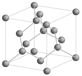
Now, this diagram is rather difficult to make sense of, and I struggled with a way to estimate the number of atoms in a given volume from that. A little more searching revealed a handy reference in a materials science textbook, however. The example I’ve linked here notes that there are 8 atoms per unit cell, which puts us in a useful position for further computation. Given that, the only remaining question is how large each unit cell is. That turns out to be provided by the crystal’s lattice constant. According to the above reference, and supported by the same information from the ever-useful HyperPhysics, the lattice constant of silicon is 0.543 nanometers. With this knowledge in hand, we can compute the average volume per atom in a silicon crystal, since the crystal structure fits 8 atoms into a cube with sides 0.543 nanometers long.
Now that we know the amount of space each atom (on average) takes up in this crystal, we can use the atomic mass of silicon to compute the density. Silicon’s atomic mass is 28.0855 atomic mass units, or about 4.66371 × 10^-23 grams.
Thus, we can easily compute the mass of a single wafer, given the volume we computed earlier.
Aside: impurities are negligible
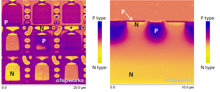
We’re going to ignore impurities in the crystal, both the undesired and desired ones. Silicon is doped to control its semiconductor properties when manufacturing integrated circuits, and these intentional impurities will affect the crystal’s density. For illustrative examples, we might refer to materials published by Chipworks, a company that specializes in reverse-engineering of integrated circuits. Below I’ve included one example from Chipworks with doped regions of the substrate annotated:
There’s also a question of the undesired impurities, but those concentrations should be even less important to our case. If we refer to some (slightly old) figures on the tolerances of a commercial wafer, well.. I’m not entirely sure how to make sense of those numbers. We can consider that the magnitude of undesired impurities in the wafer must be significantly less than that of the intentional ones (since that would affect the semiconductor properties in a hard-to-control fashion), however, and decide it’s not worth worrying about. If you look around that tolerance sheet though, you can get a good idea of how exact the mechanical specifications are. For example, local deviations in the surface must be less than 0.25 micrometers (although it doesn’t appear to include a definition for “local flatness”, rather disappointingly).
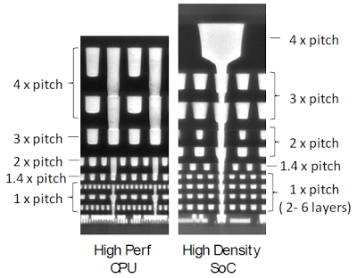
More importantly than impurities in the silicon, additional metal and insulator layers are deposited on top of the wafer for interconnection. Using material from Chipworks again, a complex integrated circuit is quite tall when considered in cross-section, mainly due to the numerous interconnects necessary:
How does this metal stack compare to the wafer’s thickness? Chipworks don’t publish many cross-sectional images like the one above, but here’s one of the same Intel 22 nanometer process featured on the left side of the above image, this time with scale bars (and much higher magnification).
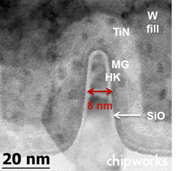
From that, we can estimate a bit from the image we have of the metal layers. It looks like the 1x-pitch metal layers are each about 40 nanometers tall, since I know that the smallest serrated-looking bits at the bottom of the stack are the FETs. Working from that, the entire interconnect stack is about (1 + 1.4 + 2 + 3 + 4) × 40 = 456 nanometers tall, assuming the metal pitch is proportional to its thickness. That’s a small fraction of the wafer’s overall thickness, which is 925000 nanometers.1
But enough of things that don’t enter into our computations. Back to the real work!
A real-world reference CPU
To this point, we’ve computed the density of monocrystalline silicon and determined the volume of a 450mm silicon wafer. Next, we should determine how many useful computing devices can be obtained from a single wafer.
As a possible model for a hypothetical processor to drive a computronium Dyson swarm, I’ll refer to Texas Instruments' MSP430 microcontrollers. These devices include an efficient CPU core with a number of analog peripherals on-chip. The analog consideration is important, because some way for the members of our Dyson swarm to communicate is required. In this situation, I’ll assume some sort of radio is on the same die (the piece of a silicon wafer that makes up a single chip) as the CPU, allowing two-way communication with nearby processors. In addition, power generation components (since these devices must gather energy from the sun independently) will likely be at least partially analog.
This assumption of radio communication is perhaps not accurate, since optical communication may be much easier to control in such a dense network, with optical emitters (LEDs or laser diodes, probably) and receivers (photodiodes) constructed directly on the wafer. For this case, however, it’s not terribly important, since space taken by unneeded analog parts on the real-world MSP430 could easily be reused, for example to provide additional on-chip memory.
With a model chip to refer to, we must now determine the size of an MSP430’s die. The smallest package (integrated circuits are usually sold encased in epoxy packages with exposed metal pads to make electrical connections to) any MSP430 is available in (that I can quickly find) appears to be a chip-scale BGA, on the MSP430F2370 (I’m providing a copy of the datasheet here, as well). This is perfect for die size estimation, since we can assume that the chip-scale BGA package (YFF in TI’s parlance) is essentially the same size as the die. This estimate is supported by a note on the package drawing (note D) that the exact package size of a device is specified in the device-specific datasheet.
Since the note indicates actual package dimensions are determined by the device contained therein, I believe it is safe to assume that the device package is approximately the same size as the die. Referring to the Device Pinout section of our datasheet, Table 2 (on page 4) provides the overall package dimensions: 3.2 ± 0.05 millimeters on each side.
Now we must determine the number of dies that can be made from a single wafer. This turns into a geometric packing problem where we want to fit as many squares (dies) as possible into a circle (the wafer), which is surprisingly hard. I found an interesting collection of records for some number of squares packed into the smallest circle, but, there’s no simple way to determine an optimal packing. Wolfram|Alpha has some capability to estimate properties of such an optimal packing, and it says we could get 15279 dies out of a 450mm wafer, with 98.37% efficiency.
But wait! We’re assuming somewhat more advanced manufacturing than is currently available. Certainly, I’d expect a computronium manufacturing effort with intent to convert the entire Solar System to recycle waste materials whenever possible, so per-wafer waste isn’t really a concern, since the portions of the wafer that cannot be made into usable dies can simply be recycled into new wafers. Thus, a simple area calculation can be used to determine the amortized number of dies yielded from each wafer.
A silicon Solar System
Now it’s time to determine how many processors we could get by converting the entire non-Solar mass of the Solar System into integrated circuits. We will assume a way exists to efficiently form the requisite materials out of what may be available, likely via nuclear fusion (particularly for converting the mostly-hydrogen gas giants into silicon).
Our first order of business, since we’re assuming all mass may be converted to be whatever elements are required, is to determine the Solar System’s mass, excluding that of the Sun itself. Wikipedia notes the following:
The mass of the Solar System excluding the Sun, Jupiter and Saturn can be determined by adding together all the calculated masses for its largest objects and using rough calculations for the masses of the Oort cloud (estimated at roughly 3 Earth masses), the Kuiper belt (estimated at roughly 0.1 Earth mass) and the asteroid belt (estimated to be 0.0005 Earth mass) for a total, rounded upwards, of ~37 Earth masses, or 8.1 percent the mass in orbit around the Sun. With the combined masses of Uranus and Neptune (~31 Earth masses) subtracted, the remaining ~6 Earth masses of material comprise 1.3 percent of the total.
Well, we could manually compute these figures, but such numbers are fairly well-known, so we’ll just ask Wolfram|Alpha what they are. It responds that the Solar System’s mass (including the Sun) is 1.9911 × 10^30 kilograms, and the Sun’s mass is 1.988435 × 10^30 kilograms. Thus the non-Solar mass is trivial to compute:
Now determine the number of dies we can make from that mass:
Final quantitative analysis
Having done all the physical computations, we finally have a sense of how a Matrioshka brain could use IPv6. We can make about 10^32 processors out of the Solar System, compared to about 10^38 (theoretically) available IPv6 addresses. That is, it would take approximately one million Matrioshka brains to completely exhaust the IPv6 address pool.
In practice, such a dense network would not be desirable, since the very large IPv6 address space allows a lot of slack in address allocation to make routing easier. For example, clearly-defined hierarchical address allocations allow routers to efficiently determine destinations for traffic via route aggregation or other methods.
Basically: once networks shift to IPv6, address exhaustion is not a concern for any forseeable future. The IPv6 address pool could support Matrioshka brains around about 1% of the stars in our galaxy (extimating about 2 × 10^11 stars in the galaxy) all in a single network. Without superluminal communication, such a network would pose its own challenges (mainly in message latency), to the point where I believe it would make more sense to have interstellar communications running on a different network that happens to be bridged with a local IP network.
I had a bit of difficulty remembering which novels I was thinking of, but Charlie Stross’ “Singularity Sky” and “Iron Sunrise” and Vernor Vinge’s “A Fire Upon the Deep” involve interesting cases where sublight shipping of information remains relevant in galactic civilizations, representing cases where (non-transcended) civilizations maintain local networks with dedicated (comparatively high-cost) links for long-range communication. I think that is a logical way to approach the problem of networking a galactic civilization, given any expected means of interstellar communication will have limited bandwidth, high latency, or both.
So what’s my conclusion? Don’t worry about IPv6 exhaustion. Even if address allocation seems extremely inefficient, since they can (in theory) be reallocated if necessary, and even extremely inefficient allocation still allows a transcended Solar civilization to function comfortably on top of an IP network.
Epilogue
Wow, that was a lot of writing. Over about a week, I spent four evenings actively writing this post, for a total of approximately 10 hours.
I wrote the math markup in this post with the Interactive LaTeX Editor, which is a really slick tool and allows me to ensure MathJax (which I use to render math markup on the site and is itself magical) will handle the expressions as expected. Highly recommended!
Anybody who finds the very lowest level of technology to be interesting (as I do) would probably do well to follow the Chipworks blogs. They also publish teardowns of consumer goods, if that’s more your thing.
As a more informed estimate, somebody who works in the semiconductor industry estimates in a talk from HoPE in 2012 that the total stackup on Intel’s 22nm process is about 100 microns, still only about a tenth of the wafer thickness. ↩︎